Design Service Introduction
Demands for high performance and low cost ICs continue to grow as we step into the deep submicron arena. Goal for meeting “Successful First Tape Out” has becoming difficult to achieve due to the increased design complexity that resulted from the shrinking transistors. The traditional approach of “one company does it all” has caused companies millions of dollars on re-tape-outs if design activities are not executed correctly. Not to mention the loss of business opportunities due to the delayed volume production.
The key ingredients for successful tape outs that enable IC or System Design Houses to meet the time to market pressure are:
- Correct design flow/methodology
- Readiness for the reliable foundries process technologies
- Availability of silicon proven IPs and libraries
EE Solutions has completed and taped out more than 800 designs over the past years. Numerous designs are in volume production since the early days when the company was founded. The successful completion of these designs requires support from multiple sources of our design partners. We have enduring partnerships with EDA vendors, IP/library vendors, and semiconductor foundries. We believe in the concept of “division of labor” and are actively searching for new partners to meet the continuous design challenges.
By working with multiple design partners, we are able to select the best tools from different tool vendors, best IPs from different IP vendors, and best semiconductor foundries that meet customers' design requirements. We have a unique “hybrid” design environment that uses tools from multiple EDA vendors plus internally developed tools for power, noise and die size optimization. We have tape out designs in TSMC, UMC, CSM, SMIC, etc. to suit customer's design/business requirements. We have vast number of IPs available in numerous process technologies across different foundries. Furthermore, by teaming up with our design partners, we are able to focus on what we do best by offering a complete integration service that enables our customers to deliver high performance solutions in multiple application domains.
Value of ASIC Solution to Customer
Value to Customer
- Cost Down (IC and BOM)
- Market Differentiation (unique solution)
- Customer Specific Solution (no standard IC or combined IC solutions)
- Product Protection (no off-the-shelf ASIC supplier)
- Product Extension (flexibility)
- Secured ASIC Supply (not dependent on IC supplier)
EES Service Types
- Provide pin-to-pin compatible solutions
- Provide multiple IC integration solutions
- Provide customized IC solutions
EES Differentiations
- Channel to Systems and IC customers in Greater China Market
- Wide selection of IP Partners and Design Partners for VASIC program
- Choices of Testing & Assembly Houses here in Taiwan & China for cost down
- Internal IP development capability
- IO and memory development capability
- Advanced Design Technologies/Methodologies
- ESD
- RTL Qualification
- Hierarchical Design Flow
- Clock/Power Methodologies
- Optical Shrink Technology (GDS2GDS design flow)
- Hybrid Design Flow – SoC Encounter, Magma
ASIC design service
As an innovator of advanced ASICs (including ASIC conversion services), EES is committed to a complete wafer design: from design recommendations, IP design and configuration, through close collaboration with your system engineers and logistics management. Wafer integration, FPGA validation, and complete back-end process and testing. We have the expertise, intellectual property (IP), and system level advantages to integrate your company's design version into an ASIC solution, whether it's a single package of monolithic wafers or multiple wafers. EES's expertise is in high reliability, low power, and low cost designs. The company can integrate IP libraries with flexible process methods to achieve a successful and cost-effective system-on-a-chip (SoC) solution.
Front-end design service
- Architecture planning
- System level simulation
- Logic design and integration
- Advanced packaging and prototyping products
Verify Component Database Design Service
- Design planning and original image synthesis
- Low power design
- Development and characterization of technical files
- Extraction and model development of synthetic component libraries
- Verilog format
EES provides various types of analog IP, and according to customer needs, the development of analog analog lines or special-purpose analog wafers. The designed chip covers power supply applications, analog signal processing, high-speed transmission signals, clock signal generation, and touch signal processing.
- Power applications: Battery Charger, DC-DC, DAC voltage and current supplies, etc.
- Analog signal processing: Sensor analog signal front-end processor, etc.
- High-speed transmission signals: LVDS, MIPI DPHY, USB 2.0, 10/100 Ethernet PHY and other interface chips
- Pulse generator: various frequency generators
- Touch signal processing: resistance, capacitance, electromagnetic touch recognition chip
SoC/Platform Based Design Service
In addition to the traditional design service offerings, we build our own solution platform not only working design database in the workstation but FPGA for system validation to shorten customers' overall design cycle. SOC design consists of a number of hardware blocks, a process core, and the embedding software that glues the entire system together. We have been working with a number of EDA partners to establish a SOC design and integration environment. We have developed a generic platform to accelerate SOC development effort. We also have established low level device drivers called BSP (Board Support Package) to accelerate the software development effort. Experienced veteran SOC designers in our team will coach you on the SOC design environment setup and upon request we will also deliver application specific platforms to accelerate your design completion.
- SMART-USB / USB 2.0 Platform
- 32-bit MCU + DSP Platform
- AI IoT Platform
- 32-bit SoC Platform (including customized S/W & H/W base on ARM cortex –M series,RISC-V, MIPS …)
- Low power SoC platform
- FPGA Verification
Design from FPGA/RTL
Upon your request, we will start our design service starting from your RTL/FPGA designs and map into corresponding physical design components, and finally deliver chip product and manage logistic for you. We will also ensure that both our logic and physical design teams are synchronized to ensure a fully functional IC on the first tape-out to enable you to perform prototype testing and fine tune your design requirements. Based on your business and design requirements, we will make recommendations on:
- Selecting the suitable foundry, assembly and testing houses
- Selecting the suitable processing technology
- Implementation/design flow from synthesis to GDS
- Logistic
Design from Netlist
Upon your request, we will start our design service starting from your design in netlist and finally deliver chip product and manage logistic for you. We will also ensure that both our logic and physical design teams are synchronized to ensure a fully functional IC on the first tape-out to enable you to perform prototype testing and fine tune your design requirements. Based on your business and design requirements, we will make recommendations on:
- Selecting assembly and testing houses
- DFT and APR
- Logistic
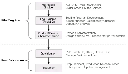
Production service Introduction
EE Solutions offers wide range of value added production/manufacturing engineering services to choose from, enabling customers to fill in the special expertise that may not be available in house. EE Solutions serves as the manufacturing partner managing fabrication, packaging, test and delivery. This offering enables customer to tap into EE Solutions in-house manufacturing engineering skills and leveraging our top tier semiconductor supply chain. This enables customers to capture many of the benefits without incurring the cost and overhead of staffing up manufacturing operations internally. EE Solutions also provides a full suite of manufacturing engineering services, as needed, including package selection and design, test program development, Silicon Validation, Failure Analysis, and new product qualification.
Why choose EES as a Turnkey partner?
- Provide Competitive Cost Solution
- Design / Manufacturing Infrastructure in China
- Supply Chain (Foundry/Assembly/Testing/FA) - Production Proven of Turnkey Flow
- Mask tape out, Wafer Process, Assembly, Testing Program Development, Device Validation &
Characterization - Experienced Supply Chain Management
- Experts from Wf foundry, Assembly, Testing house & Production Control
- Vendor Qualification flow, Drop Shipment, WIP, Schedule Control
What we can provide?
Production Proven of Turnkey Flow

Fabrication
EE Solutions partners with world class foundries to provide complete manufacturing services. EE Solutions staff brings years of Semiconductor manufacturing experience and product engineering experience to every engagement. We work closely with our customers to select the right process and technology solution for their designs. This requires careful comparisons between different foundries, objectives and target price. Our manufacturing engineering staff keeps abreast of the changes and stays current with all existing and new technologies to ensure complete choice.
EE Solutions provides a unique service that delivers fast, inexpensive IC prototypes with special features not provided by foundries. Currently foundries require purchasing a complete mask set or consist of multi-project wafer services with limited package and test options. Since only a limited number of standard packages are available with multi-project wafer services, customer must settle for bare, unpackaged and untested die.
EE Solutions offers complete integrated IC prototyping service that can deliver any thing from bare die to packaged, fully tested parts. In this option, EE Solutions supports full complement of packages including custom packages. In addition we can perform basic electrical and functional tests.
Partner
|
|


Package & Assembly
As device geometries shrink, semiconductor assembly process becomes more complex. Increasing the severity of this complex problem is the increasing diversity and sophistication of microelectronics that requires a greater variety advanced package types.
EE Solutions understands the importance of selecting the proper packaging solution to meet the technical and cost constraints of each design. Our packaging engineers bring in years of packaging experience and gets involved early in the design cycle. We work with our customers to evaluate the package options (BGA, Lead Frame, Flipchip and SIP/MCM) that are best optimized for the application requirements of the design. Our engineers work very closely with design engineers to ensure substrate design meets product specification.
In order to address these packaging challenges, EE Solutions recognizes the need for relationships with firms that offer full complement of packaging and test solutions and services. Further more proximity of these top tier firms creates a seamless working environment between two engineering groups which result in a much faster resolution of issues. All our partners are located in Taiwan and China and have strategic relationships with ASE, TSE, TICP in packaging and Assembly area.
Partner


Test Development
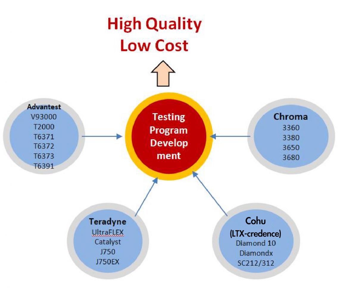
EE Solutions provides test planning and strategies for digital, analog and memory blocks and work with customers to select the right test platforms to optimize costs. Our engineers have extensive experience with top tier testing firms in Taiwan. We design load boards and probe cards and provide test program development for all major platforms (Advantest, Teradyne, Cohu (LTX-credence) and Chorma). We have proprietary test pattern conversion tools support all the major platforms. EE Solutions experienced engineers determine the most cost effective production tester based on the required pin count, speed, and nature of the design. All our testing partners are located in Taiwan and have relationships with vendors like ASE、SPIL、KYEC、Chipbond、 PAT、GT 、 YTEC, makes it efficient to resolve issues.
Provided variable platform to meet:
Successful Cases
|
Application |
Package Type |
Challenge/Character |
Tester |
|
Communication |
LQFP64 |
Analog Circuit |
Teradyne Catalyst |
|
4CDSP |
Parallel Testing |
||
|
(cost down version) |
|||
|
Communication |
PBGA |
Digital Circuit |
HP 83000 |
|
Controller-WCDMA |
High Pin Count |
||
|
Communication |
HSBGA |
Digital Circuit |
HP 83000 |
|
Controller-WCDMA |
High Pin Count |
||
|
System Controller |
CSBGA |
Digital Circuit |
Teradyne J750 |
|
High Pin Count |
|||
|
(cost down version) |
|||
|
System Controller |
HSBGA |
Digital Circuit |
Teradyne UltraFLEX |
|
High Pin Count/LVDS |
Partner


Yield & Failure Analysis
Primary responsibility of our Product Engineering group is to maximize yield from each wafer. EE Solutions monitor yields and work closely with both the foundry engineers and assembly house to maximize the yield in order to get the best possible cost to our customers.
EE Solutions offers a full range of quality services for the entire product life cycle. Yield optimization services include yield analysis, corner lot characterization and process re-targeting. We assist customers during the validation and debugging phase by providing benchmark measurements. EE Solutions provides die and packaging qualification including burn-in, ESD, latch up and high accelerated stress test.
We provide complete support to new products including new product qualification, sophisticated failure analysis and optimization.
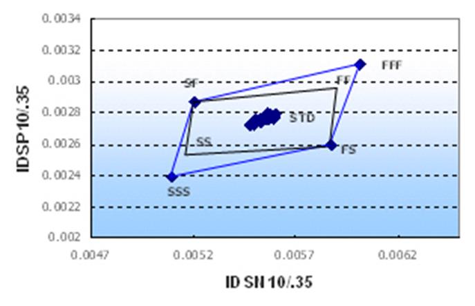
The skill of yield improvement
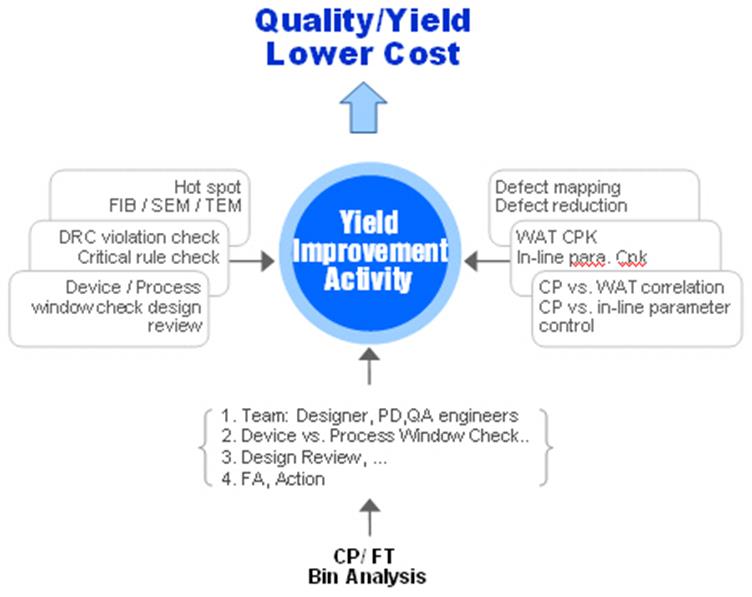
Design Window vs. Process Margin Check
Product Reliability Qualification
- Reliability Qualification Requested by Customers
- Qualification Plan, Sampling Size, Items
- Base on Customer Plan
- Ref. on the Industrial Standard
- Reference From Assembly House - Provide the Reliability Report
- Date Analysis and Suggestion - Provide the Failure Analysis & Corrective Action
Total Solutions on Reliability Test
|
Test Item |
Test Condition |
Readout (Hour or Cycle) |
Test Method |
|
Operating Life Test (OLT) |
Ta = 125℃, .3*Vcc |
168/500/1000 (HR) |
MIL-STD-750C |
|
Pressure Cooker Test (PCT) |
Ta = 121℃ |
48/96/168 (HR) |
MIL-STD-19500E |
|
Moisture Resistance |
Ta = 85℃ |
168/500/1000 (HR) |
MIL-STD-750C |
|
Temperature Humidity test (THT) |
Ta = 85℃ |
168/500/1000 (HR) |
JEDEC22-A101-B |
|
Temperature Humidity with Bias Test (THBT) |
Ta = 85℃ |
168/500/1000 (HR) |
JEDEC22-A101-B |
|
Thermal Shock Test (TST) |
-55℃/5mins to 150℃/5mins |
100 CYC |
MIL-STD-750C |
|
Temperature Cycling Test (TCT) |
-55℃/15mins to 125℃/15mins, |
500/1000 CYC |
MIL-STD-750C |
|
High Temperature Storage Life |
Ta = 150℃ |
168/500/1000 (HR) |
MIL-STD-750C |
Total Solutions on ESD, Latch-up Test
|
Test Item |
Test Condition |
Readout (Hour or Cycle) |
Test Method |
|
Electrostatic Discharge (ESD) |
Ta = 25℃, RH < 55%, |
VSS (±) |
JESD22-A114-B |
|
Latch-Up |
Ta = 25℃, |
+Voltage Trg –Voltage Trg |
EIA/JESD78 |
|
ELECTRO MIGRATION (EM) |
Follow JEDEC |
- |
>1.0 mA/um JESD63 |
|
Solder ability |
Ta = 215 ± 5℃ |
Dipping 5sec |
MIL-STD-750C |
Total Solutions on Failure Analysis
- Electrical Analysis
- Curve Tracer, Logic Analyzer,
- Signal Generator
- HP 4145, 4156 - Package Level Analysis
- X-ray, SAM
- De-cap, Dry Plasma Etched - Leakage Current Analysis
- EMMI, Liquid Crystal, Hot Spot
- O Birch - Physical Analysis
- SEM, TEM, FIB, u-scope
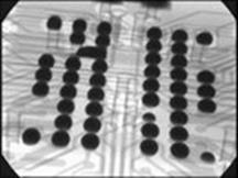
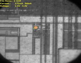
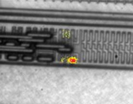
Failure Analysis
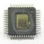
(1) X-ray Analysis
|
|
Golden wire / Ball Analysis |
|
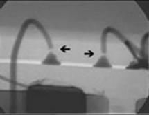
(2) De-Cap Analysis
|
|
Passivation Layer, Top side review |
(3) Emission Analysis
|
|
|
(4) SAM
|
|
|
Post Fabrication
For customers already purchasing wafers, EE Solutions can complete the path to finished IC’s with the comprehensive package, test and other services listed above.
The result is a complete end-to-end solution for custom chip manufacturing and delivery, including all post fabrication supply chain management.
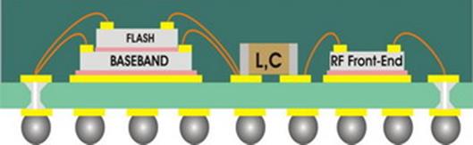
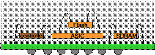
SIP Solution
EES had successfully developed the SIP (MCM) solutions for our customers achieving the high device performance, smaller package size and lower cost. There are several solutions be used by difference package types, which include the BGA, QFP and WCSP with Side by side, Stack Dies solutions.
|
Product |
Package Type |
Body Size |
KGD |
|
DTV |
TFBGA196 |
12*12 |
ASIC, AFE, SDRAM |
|
Security Camera |
TFBGA169 |
11*11 |
ASIC, Flash, SDRAM, Conroller |
|
Metrology |
QFP216 |
24*24 |
ASIC |
Success Case 1:
- Application: DTV
- Package Type: LFBGA 208, 12mm*12 ^mm
- Die Structure: 3 Dies Package ( Stack Dies + Side by Side)
- Die Information: EES002 + eFlash + AFE
|
|
|
|
|
|
|
|
|
|
|
|
|
|
|
|
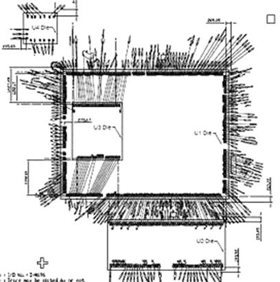
Success Case 2:
- Application: Security Camera
- Package Type: LFBGA 169, 11mm*11 ^mm
- Die Structure: 4 Dies Package (Stack Dies + Side by Side)
- Die Information: EES002 + eFlash + SDRAM + Controller
|
|
|
|
|
|
|
|
|
|
|
|
|
|
|
|
|
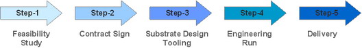
Step 1: |
Provide Chip Information |
|
Step 2: |
Contract Sign |
|
Step 3: |
Starting Substrate Design ( 2 ~ 4 weeks) |
|
Step 4: |
Engineering Run |
|
Step 5: |
Delivery |
- EES participate the design quality checking though several state-of-art methodology to insure the best quality of the result chips.
- The design quality checking includes: Code purification, netlist checking, pin-ball assignment check, design power calculation, low-power design, cycle-base pattern translator.
- Several methodologies were deployed to insure the best high-quality and low-cost chips.
- Power integrity flow: Design for low power
- Signal integrity flow: Signal integrity effects handling
- Nanometer design flow: Nanometer physical/electrical handling
- Optical shrink technology: Cost down by optical shrink process
- ESD quality check/design: Whole chip ESD protection design methodology
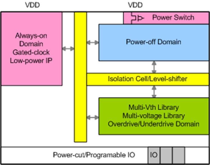
- EES Low-Power design flow provides users with a complete front-to-back methodology for low-power implementation and verification platform. It contains low power IPs with low power design methodology for Power Switch, Multi-supply/Multi-voltage, Multi-Vt library and gated clock implementation.
- Those methodologies help to achieve the lowest leakage/standby/dynamic power.
- Leakage/standby current: < 1.0 uA
- No performance degradation
- Easy power up procedure handling
- Better IR result/consistent IR control
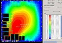
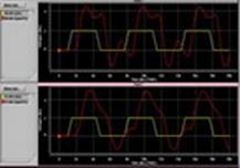
Perform Static IR analysis, Dynamic IR analysis, SSO analysis/prevention.
|
|
|
- Static IR/Dynamic IR analysis
|
|
|
- SSO Analysis
|
|
|
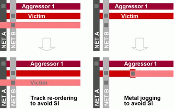
- EES signal integrity design flow provides users a complete design quality insurance of physical/electrical effect on nanometer device.
- High accuracy noise library include ac/dc noise margin prepare by spice simulator.
- Timing analysis considering the delta delay induced by cross-talk noise.
- Correct-by-construction noise prevention flow through
- Automatic routing optimization to reduce coupling capacitance on critical nets
- Load insertion on victim net to reduce coupling cap ratio
- Track re-order/metal jogging
Nanometer Design Flow
Several analysis flow and prevention mechanism were deployed to handle those nanometer design:
- OCV (On Chip Variation) analysis
- Multi-corner RC conditions handling
- Multi-mode constrains timing optimization
- Advance DFT: Scan Compression, at-speed Scan , Auto MBIST integration
Optical Shrink Technology
EES has developed a unique process migration flow for large die-size products or high volume products. This flow will allow customers to have a "cost down" version of their original design and will not require extra manpower to complete the new design.
ESD Quality Check/Design
- Superior ESD protection design method for I/O cell
- Superior whole chip ESD protection design methodology
- Design for multi-power domain
- Design for multi-analog/digital domain
- Relationship between ESD level and the distance of power/ground to signal cell
- Design for high voltage tolerance I/O cell
- Embedded clamp circuit
- Good discharge paths
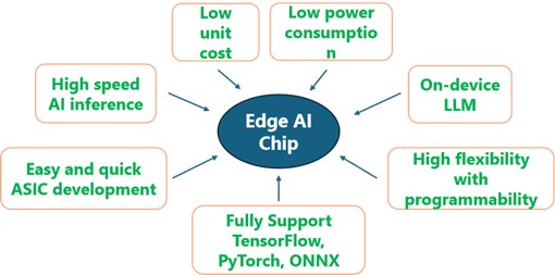
General Purpose Edge AI IP / TPU (GPTPU)
- GPTPU: By combining the ASAP platform with a novel tensor core, this solution delivers optimal tensor performance—especially for LLMs
- High Performance: GPTPU is highly optimized for processing large matrix in LLMs using on-chip tensor network, which can scale to Peta flops in one chip.
- Low Power Consumption: It can achieve a power efficiency of 8–20 TOPS per Watt using only a 22nm ASIC node, without relying on the most advanced process technology.
- Cost Efficient: The domain-specific accelerators in GPTPU achieve the same performance as GPU with at least 10x smaller area.
- Flexible/Programmable: ASAP architecture can reuse domain specific accelerators and shared accelerator Cache using flexible and low latency instruction scheduling. Therefore, it is programmable to adapt to improvements in AI models and switch to different models within the same AI domain—even after the chip being tape-out.
- GPTPU: Ideal for Edge AI
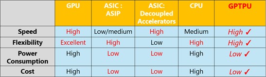
- GPTPU: Ideal for Edge AIASAP: It combines the advantages of ASIP and decoupled accelerators. It also allows designing advanced AI chips using high-level languages like C/C++ with quick turn-around development time.
- GPTPU: Combining ASAP platform with the novel tensor core enabling the optimum tensor performance, especially for LLM . High performance and flexibility but 10x higher power or cost efficiency than GPU.